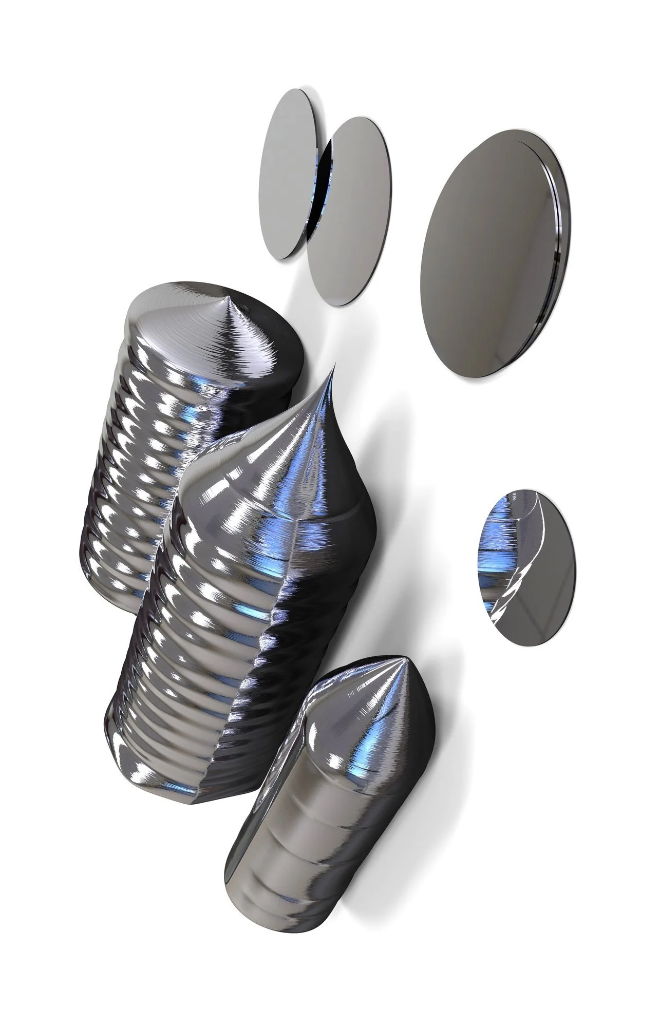
Silicon Wafers
Camera: Canon Eos R8
Lens: Canon RF100-400 F5.6-8 with 27mm extension & Raynox DCR-250
In this post I will try to explain the process used to create these intricate discs
The wafers start as a very large and incredibly pure (99.9999%) silicon crystal known as a “boule” or “ingot”. It is then sliced very thinly into individual wafers using a thin wire coated in diamond dust.
These wafers are then finished in a lapping machine, which more or less just grinds the surface of wafer into a perfectly flat surface, ensuring the two surfaces are perfectly parallel as well as the exact specified thickness.
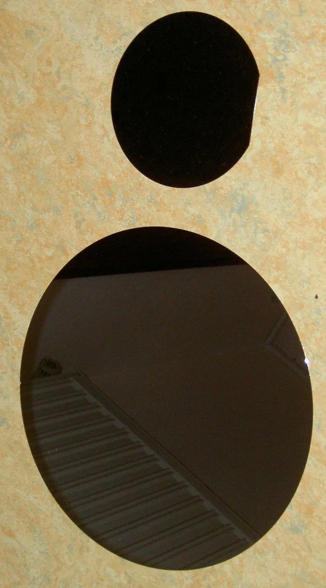
At this stage the wafer is nearly the perfect size, however requires chemical cleaning and polishing to reach a mirror like finish with no surface imperfections.
Once finished the wafer is very carefully stored to prevent any dust particles from landing on them. These wafers must remain perfect for the following processes to work.
From that point the process becomes more intricate and technical, very small changes are made to the crystal structure to alter its electrical properties. Thin films of differing materials are deposited onto the wafers surface, these can do a variety of things depending on material used, however that knowledge is beyond my understanding at the time! Finally a photoresist layer is added to the wafer. This layer responds to light being applied to it, usually hardening the portions exposed to light and allowing the areas not exposed to be washed away easily.
The wafer is then processed by a very high energy ultraviolet laser in order to etch the design into the photoresist applied earlier, these designs are of the smallest imaginable and require an incredible level of precision. The light is passed through a slightly larger negative of the chip design being made, this allows the photoresist to only harden in the correct areas as well as the design to be “shrunk” slightly due to the way the light passes through it.
After the photoresist has been hardened in the proper areas the wafer is removed and sent to be etched, this process strips away the unhardened photoresist as well as the deposited material below it, preserving the details created by the laser in the prior step and forming the chip’s electrical systems. The exposed silicon is then bombarded with specific ions to change its electrical properties, another step that reaches the end of my knowledge on the subject!
This entire process may need to be repeated several times to develop all of the interconnecting layers of the chip. Some memory chips require stacking up to 175 layers of designs, this means the process must be repeated 175 times in those cases. Adding a massive amount of work and cost.

Once finished the end result looks something like this, with many identical chips laid out on the wafer. Some companies will still use the outer rims of the wafer to create a portion of a chip. These are non functional but do serve as a quality check, as you can inspect what was made for any possible flaws or errors in the process. Each chip is inspected, either electrically by actually running the chip with a specialized testing robot, or by optically inspecting it with a similar robot.
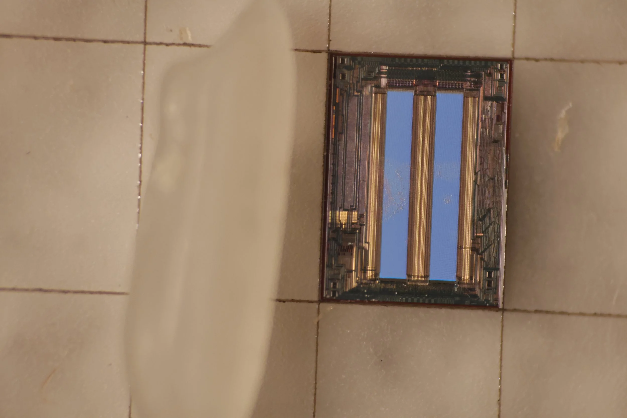
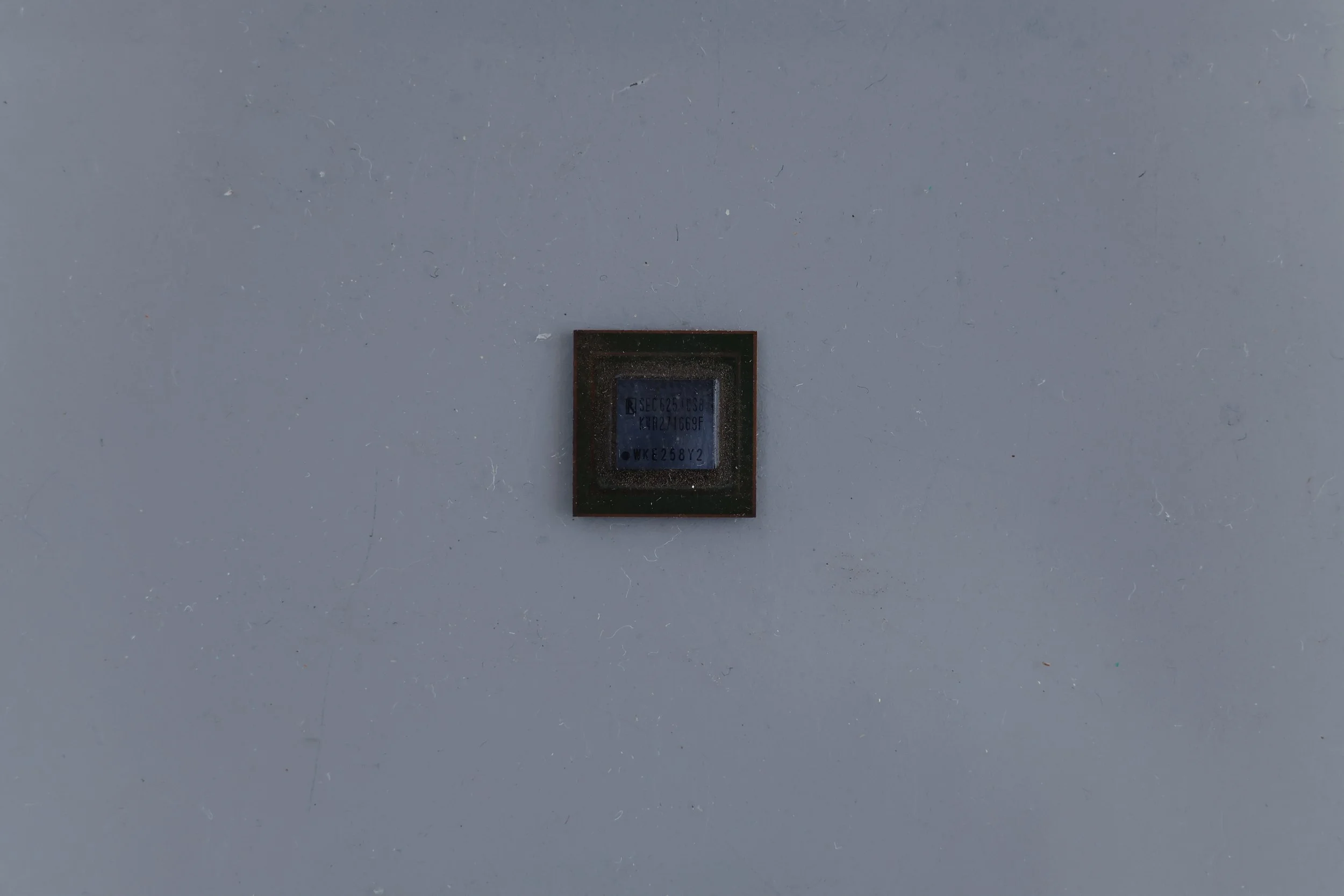
This chip is sitting beside a single grain of rice, showing the incredible detail in such a small bit of silicon.
Assuming the yield from the wafer is profitable they are then carefully diced into their respective chips. At this stage the process is more or less complete, and only requires packaging into usable cases for product designers to use for their electronics.
The following shots are various examples of how the chip can be packaged, these were taken from old electronics I had lying around, and I wasn’t the most delicate getting them apart, so most have damage in places. However you can see how the silicon chip is added onto a small circuit board to make it easier to use in designs and to protect the fragile silicon, Ill explain how they are electrically wired below.
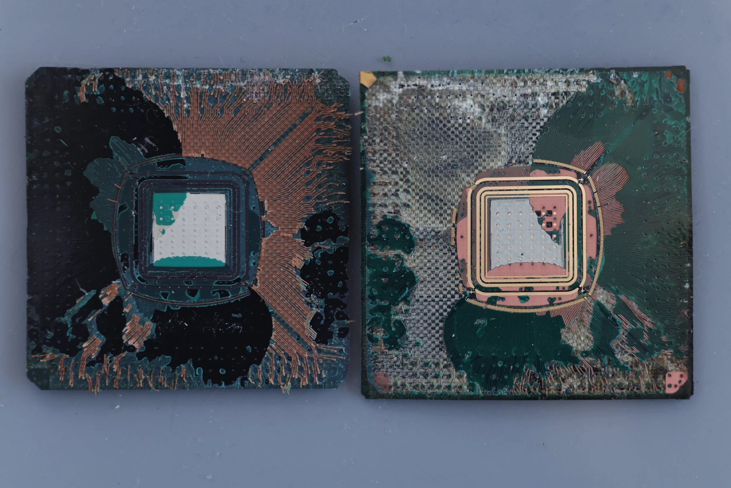

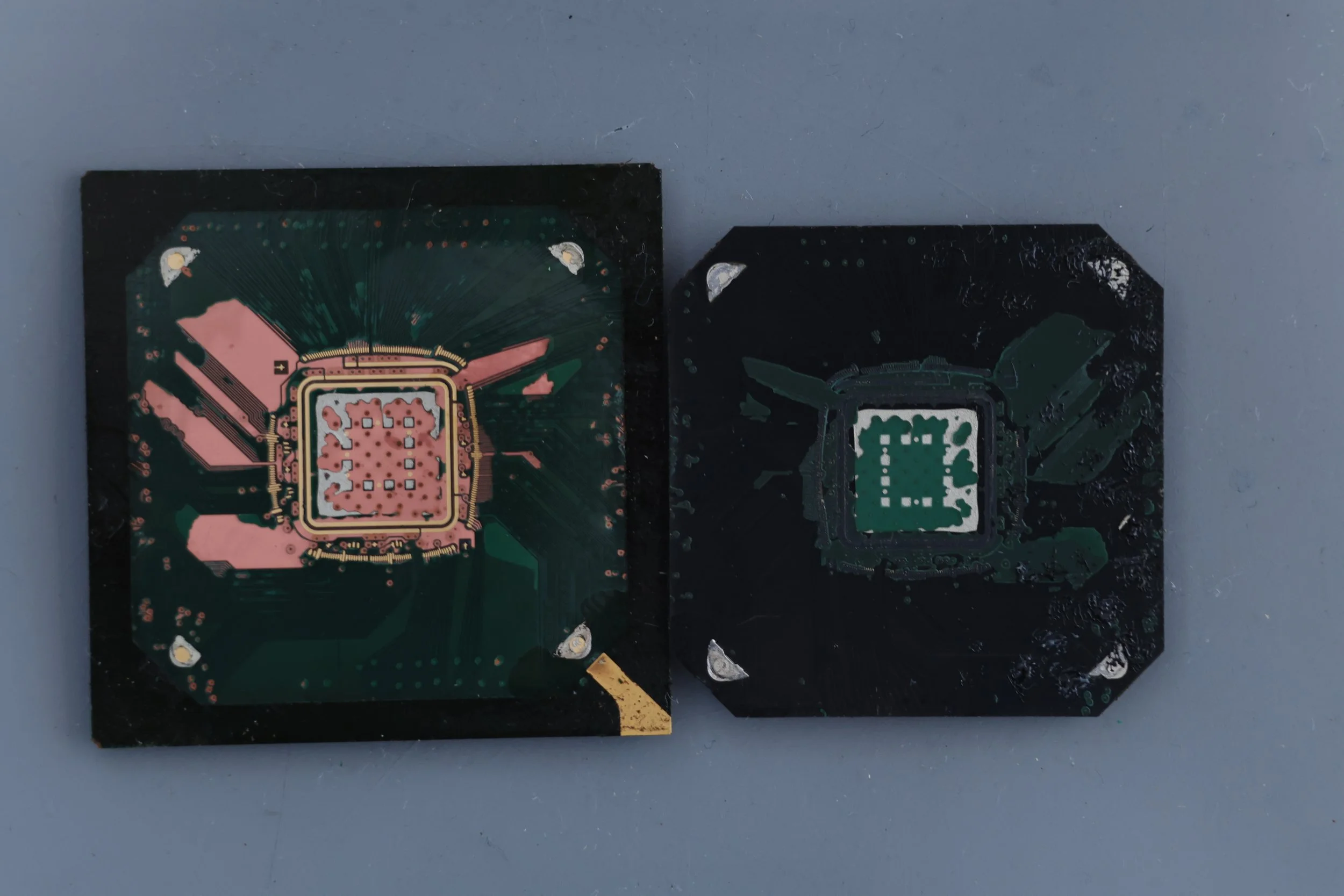
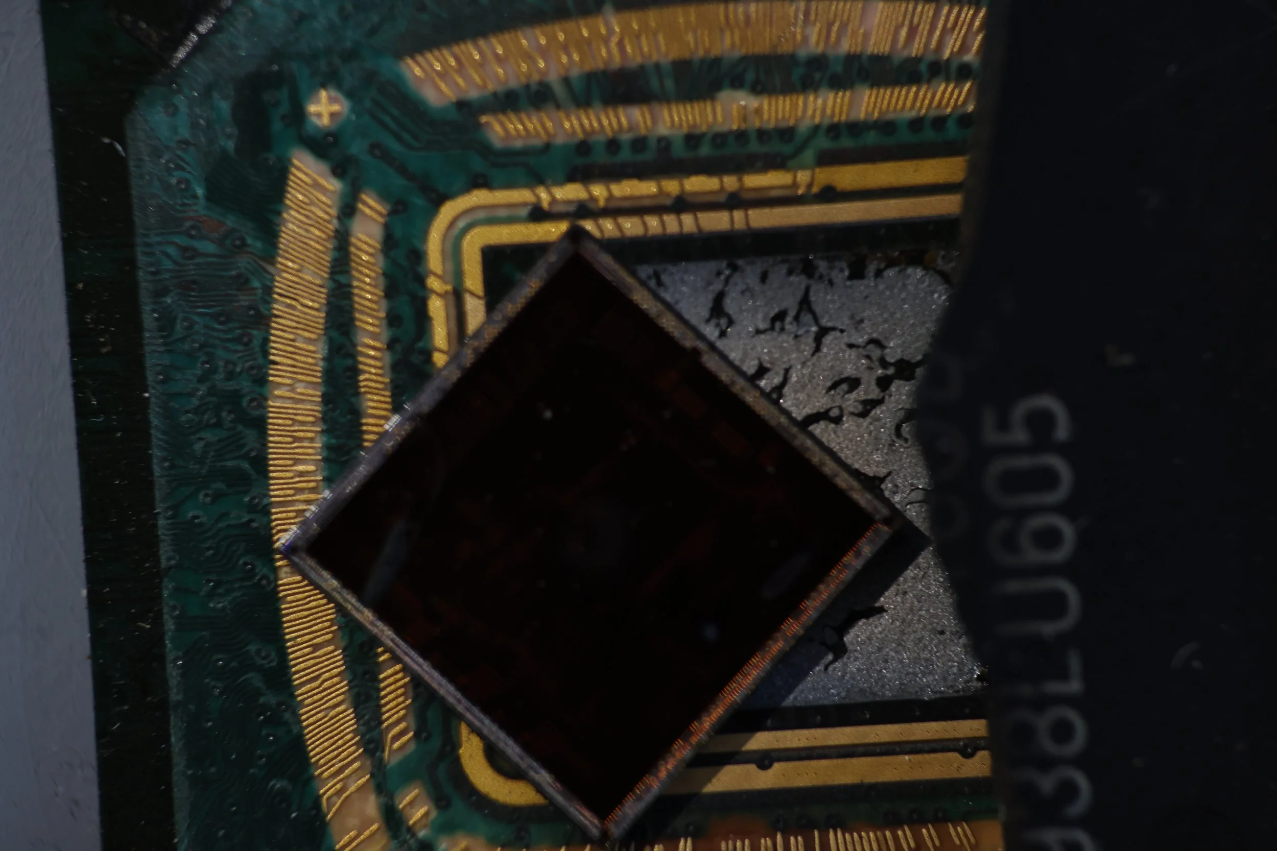
In this case I was able to get the silicon chip to actually come out of the plastic housing mostly intact. The many little gold spots each had a tiny gold wire, known as a bond wire, welded to it and a specific point on the chip. There can be thousands of these incredibly fragile wires running to the chip, this is why it is essential to put them in a casing of some kind, usually plastic or metal. Some chips don’t require bond wires as they are designed to use the silicon surface as the contact points, an example is near the bottom of this post.
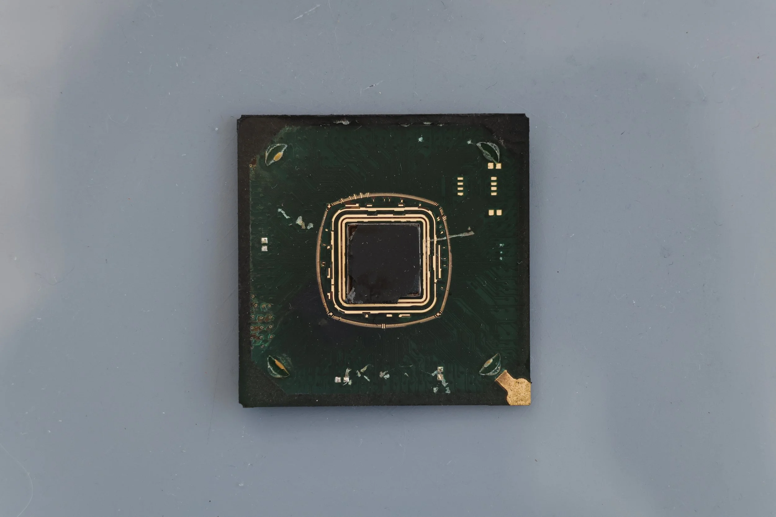
In this photo you can see portions of the green solder mask pulled from the board revealing the copper below, the solder mask is only there to protect the copper surface of the circuit board.
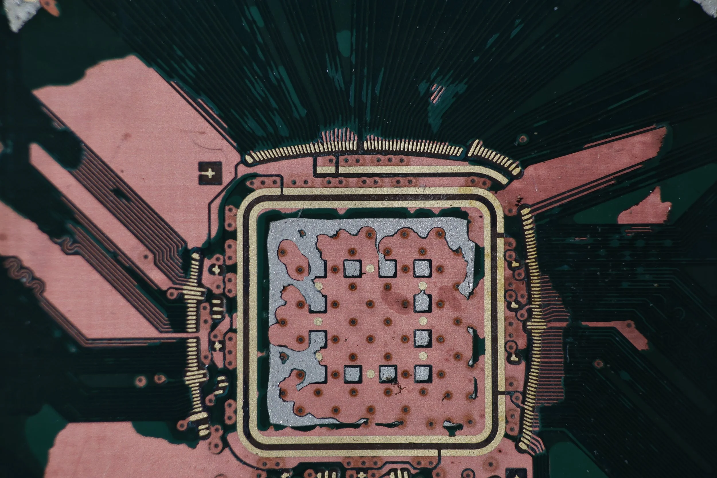
However with the solder mask removed it is much easier to see the fine details and traces of the copper. The center square with gray still visible is where the chip would sit, the gray material is a thermal compound to transfer heat away from the silicon and into the copper.
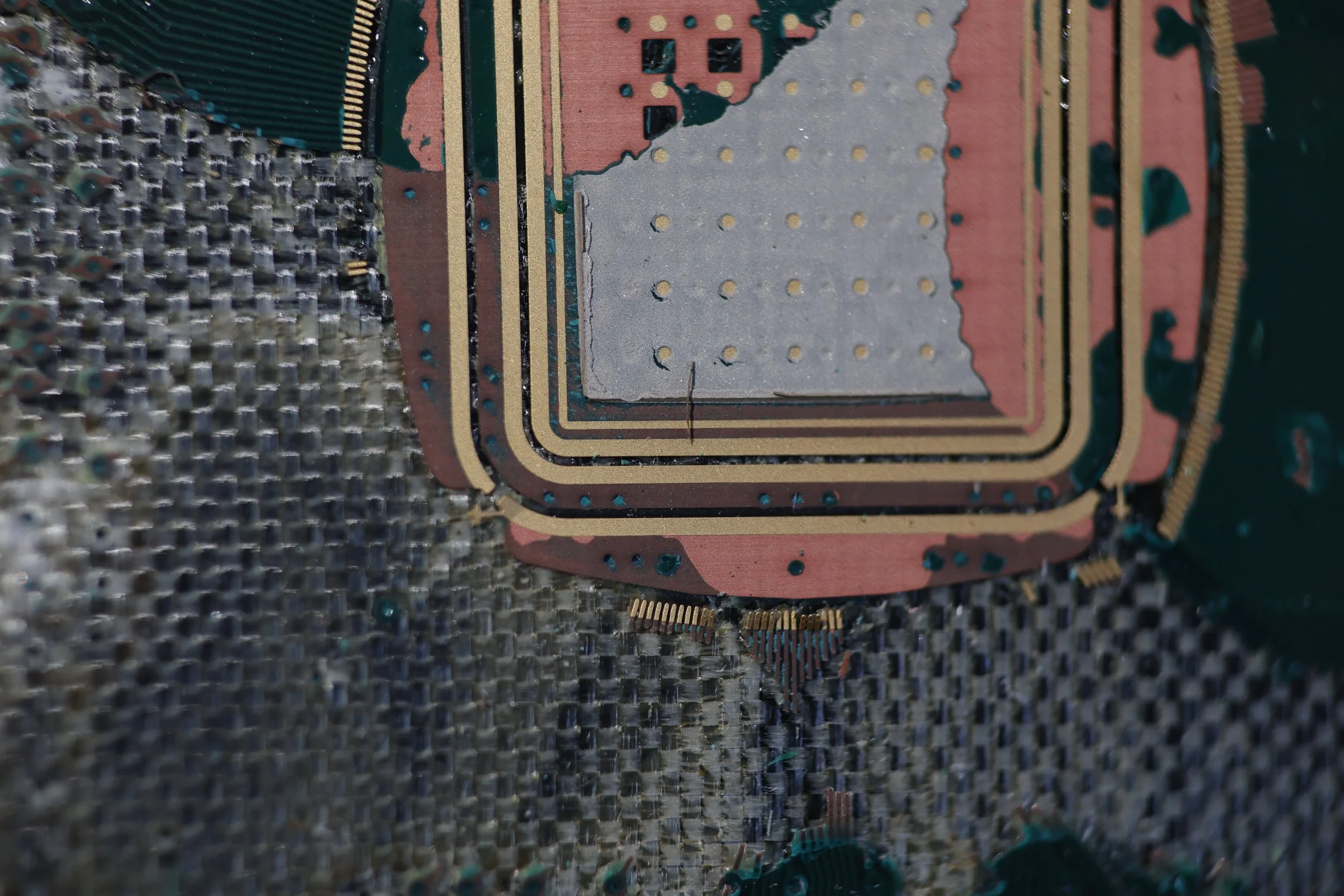
While removing the plastic casing on this one I damaged the board a bit more, revealing the woven fiberglass circuit boards are made of. Not all are made this way however this is by far the most common. It provides a strong and non-conductive base to build on. Discussing circuit boards is a topic for a whole other post on its own, as the entire process is a lot like the process of creating silicon wafers, however a much larger scale.
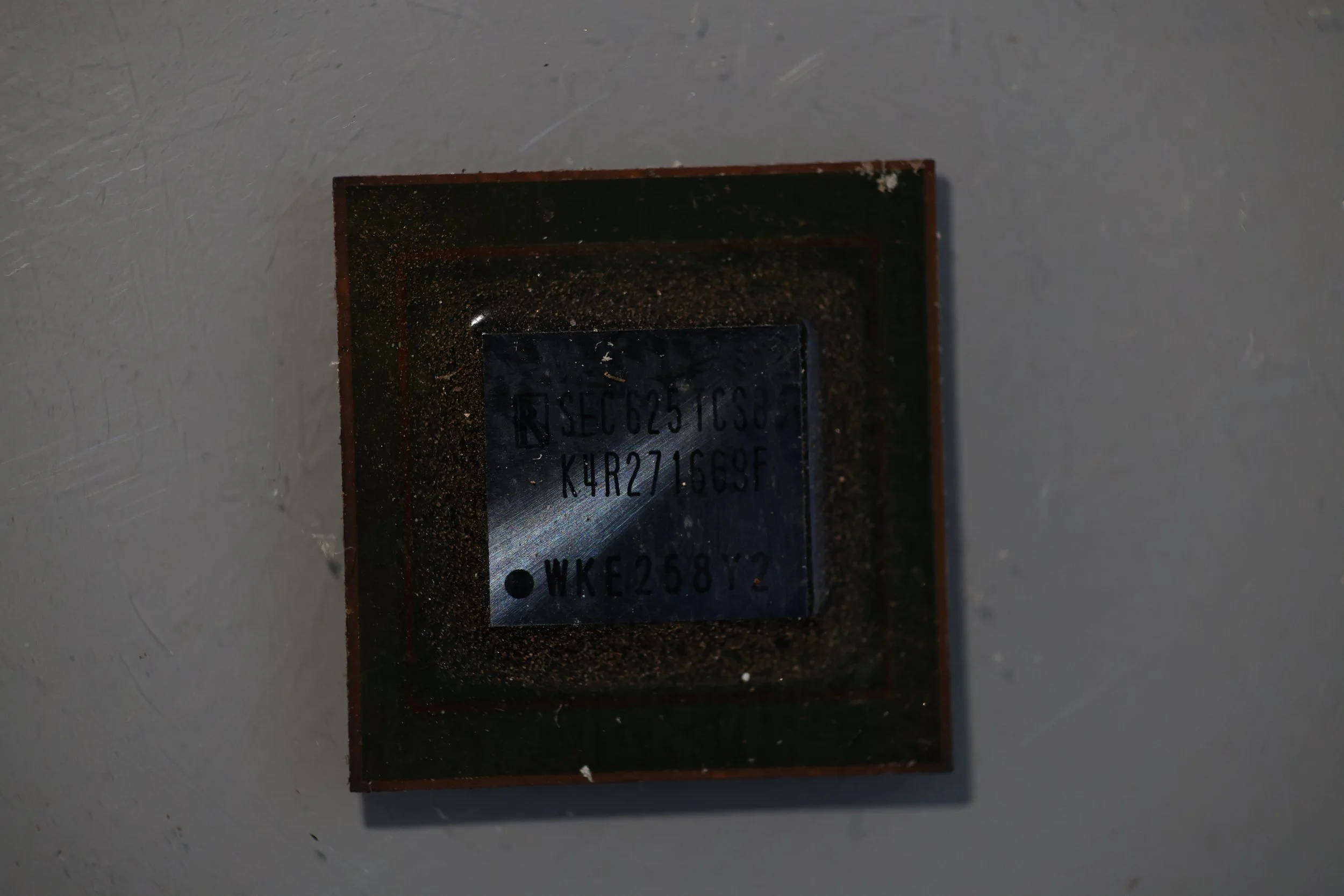
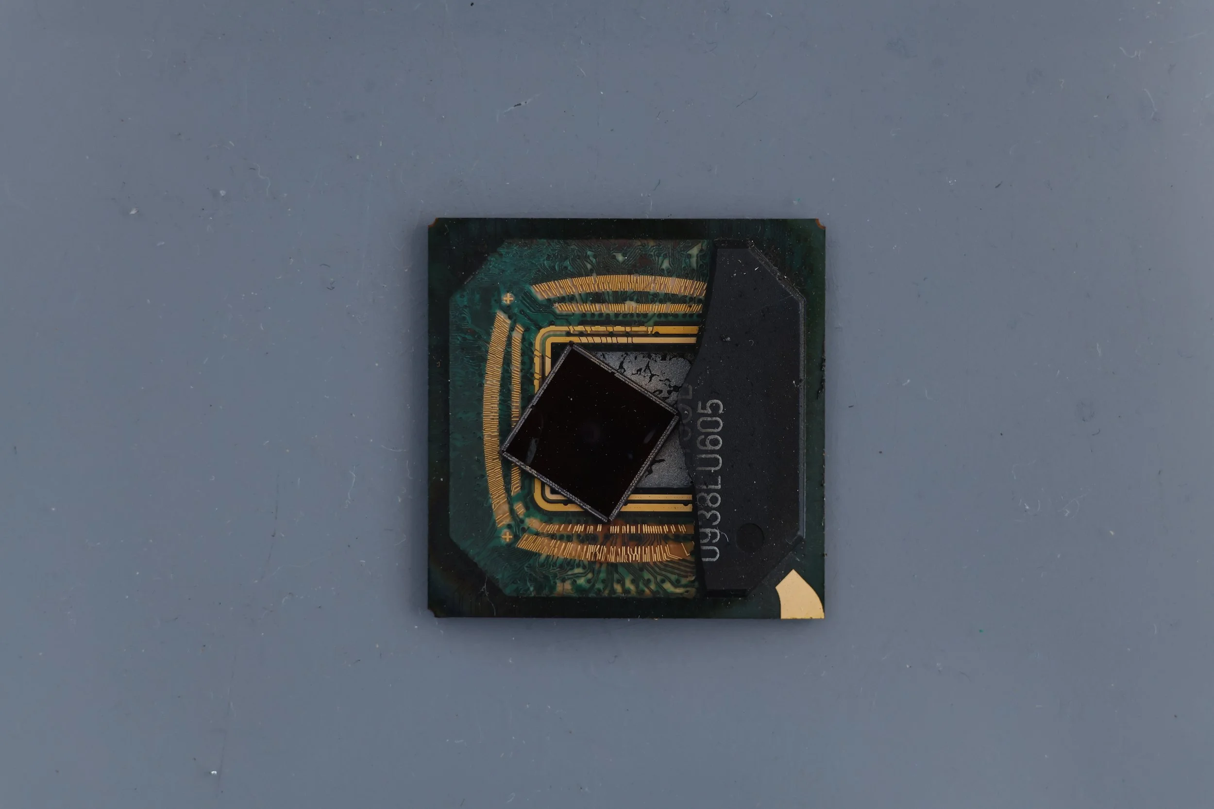
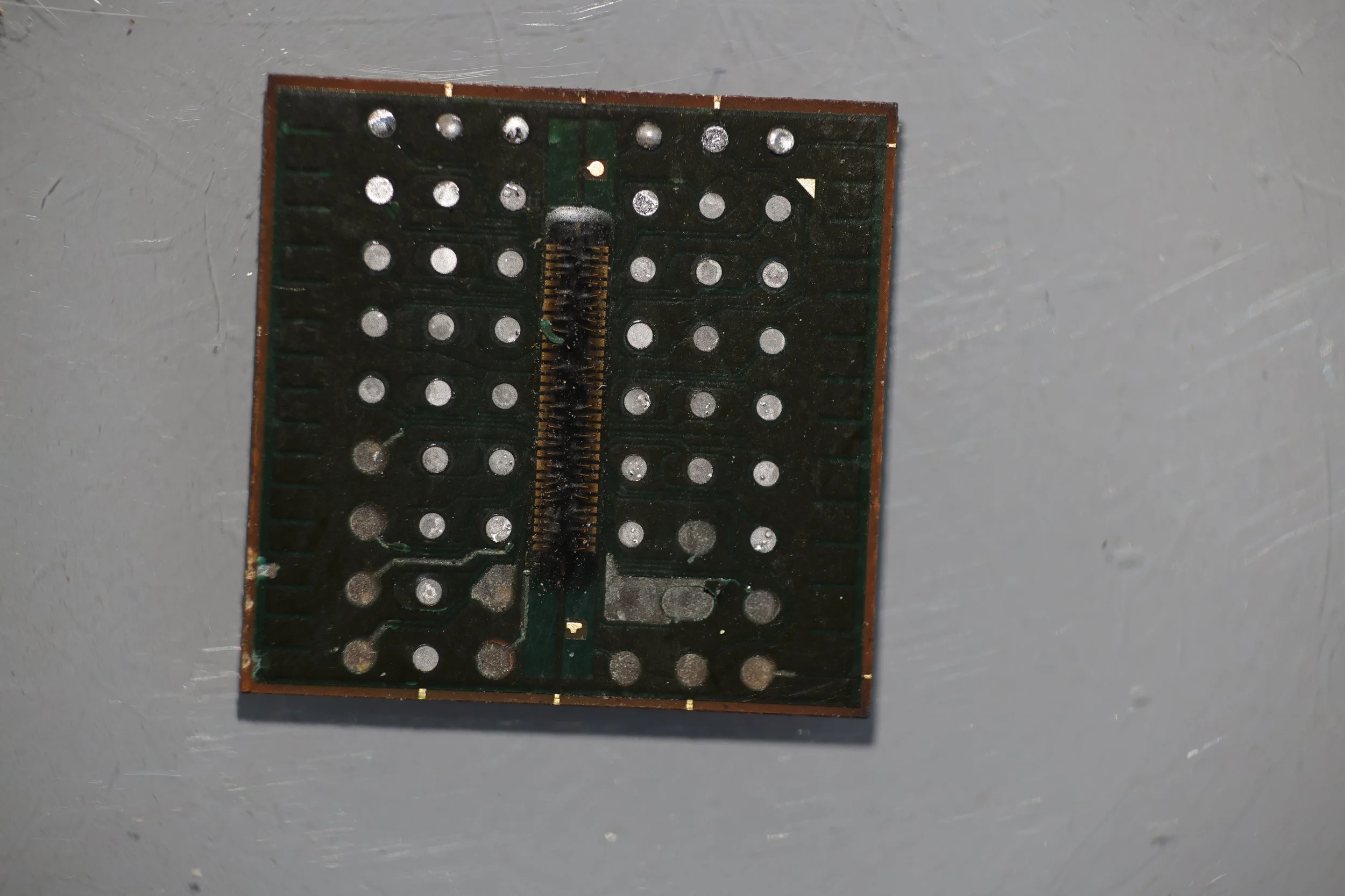
This was the simplest package I found in the devices I had to take apart, this is simply a chip upside down to allow the etched surface to act as the bond wires, removing a complicated and costly step from the process. This however only works for chips with a limited number of contacts as they have to be larger than the bond wire welding points.
The below image shows the underside of this chip, the little silver spots are electrical contacts that were soldered to the circuit board to allow it to work!
I think that about wraps it up! I don’t know the entire process by heart, but do know the general steps, I don’t think I forgot any steps but I’m sure I forgot some little detail!
I hope this little explanation may have taught you something, and wasn’t too hard to follow. If any parts could use some more clarification feel free to let me know at my email below. I’d be happy to do more research and attempt to explain it in an easier to understand way! Thanks for reading!